





Negative power supply rails are fundamental pillars of modern electronic system design. While positive rails dominate the power delivery conversation, negative supply voltages are vital across a wide spectrum of industries. They provide essential bias, wide signal swings, and precise operational ranges for complex analog, digital, and power-switching architectures.
As electronic systems push for higher densities, faster switching frequencies, and tighter noise margins, generating reliable negative rails becomes an intricate engineering challenge. Written by Rakshith Prasad Shashibhushan, a Senior Product Applications Engineer in the High-Performance Power Group at Analog Devices Inc. (ADI), recent technical insights emphasize that designing an optimized voltage-loop compensator is critical for buck-boost converters generating negative voltage rails.

This comprehensive guide explores the structural nuances, small-signal modeling, and compensation design methodologies necessary to build stable, fast-transient inverting buck-boost (IBB) power supplies.
The Ubiquity and Necessity of Negative Rails
To understand why precision compensation is required, one must first examine where and why negative voltage rails are deployed.
In automotive electronics, negative supply rails are indispensable within gate-driver circuits. Modern electric vehicles (EVs) rely heavily on wide-bandgap (WBG) semiconductors, such as gallium-nitride (GaN) field-effect transistors (FETs) and silicon-carbide (SiC) MOSFETs, integrated into onboard chargers (OBCs) and traction inverters. Applying negative gate-drive voltages ensures fast, efficient, and secure switching, preventing false turn-ons and minimizing switching losses.
In industrial and medical instrumentation, precision analog front ends (AFEs) utilize negative rails alongside positive ones to form symmetrical power supplies. High-resolution analog-to-digital converters (ADCs), digital-to-analog converters (DACs), and rail-to-rail operational amplifiers require these negative supplies to maintain a full dynamic range, excellent linearity, and low distortion. Furthermore, medical imaging hardware relies on stable negative voltages for accurate detector biasing and precise signal conditioning.

Data centers and telecommunication networks also lean heavily on negative supply architectures. Optical transceivers apply negative bias voltages to high-speed photodiodes, which translate incoming fiber-optic light pulses into electrical data streams for high-speed servers and network switches. This negative bias is crucial for achieving high-speed responses and ultra-low-noise operations. Finally, high-resolution consumer LCD displays employ negative voltages to control individual pixels and fine-tune contrast ratios.

Topologies: Dedicated IBB Regulators vs. Reconfigured Buck Converters
Engineers typically generate these mandatory negative rails using the inverting buck-boost (IBB) topology. Two primary implementation paths exist:

- Dedicated IBB Solutions: Utilizing a buck-boost regulator specifically engineered from the ground up for negative-output operation (such as ADI’s MAX17577, illustrated in Figure 1).
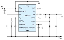
- Reconfigured Buck Regulators: Taking a standard, highly integrated buck regulator and rerouting its power stage to output negative voltages (such as the LT8624S configured as an inverting buck-boost, illustrated in Figure 2).
Each approach presents specific trade-offs regarding component stress, efficiency, thermal performance, and control complexity. To navigate these trade-offs successfully, power supply designers must execute a rigorous, step-by-step power-stage design followed by careful small-signal compensation.

Step-by-Step Power-Stage Design Procedure
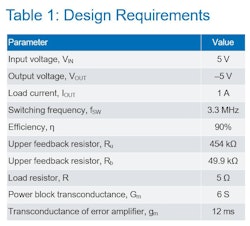
Developing a reliable small-signal control-to-output transfer function requires working under peak current-mode control operating in continuous conduction mode (CCM). The design workflow starts by establishing baseline electrical requirements—such as input voltage ($VIN$), output voltage ($VOUT$), maximum load current ($IOUT$), and switching frequency ($fSW$).

1. Duty Cycle Calculation
The steady-state duty cycle ($D$) for an inverting buck-boost converter operating in CCM is calculated using the input and output voltages, accounting for diode or synchronous rectifier forward voltage drops ($V_D$) if applicable:

$$D = fracVOUTVIN + $$

2. Inductor Peak Current Estimation
Assuming an AC ripple current target of roughly 30% ($0.3$) of the average inductor current, the average inductor current ($IL$) and peak inductor current ($IL,peak$) are determined via:

$$IL = fracIOUT1 – D$$

$$I_L,peak = I_L times left(1 + frac0.32right)$$

3. Inductor Selection and Minimum Inductance ($L_min$)
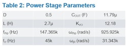
The chosen inductor must feature an RMS current rating ($I_RMS$) greater than $IL$ and a saturation current rating ($ISAT$) exceeding $I_L,peak$. The baseline required inductance is calculated as:

$$L = fracVIN cdot DfSW cdot Delta I_L$$
For buck converter ICs deployed in IBB mode where the duty cycle exceeds 50%, the selected inductance must clear a minimum threshold ($Lmin$) defined in the device datasheet. For components like the LT8624S, the formula is adapted by replacing $VIN$ with $VIN + |VOUT|$ and incorporating the calculated duty cycle:

$$Lmin = frac) cdot (1 – D) cdot VOUT dots[textDatasheet Specific Parameters]$$

4. Right-Half-Plane (RHP) Zero Determination
A critical phenomenon in boost and buck-boost topologies is the presence of a right-half-plane (RHP) zero in the control-to-output transfer function. The frequency of the RHP zero ($omega_z,RHP$) is dictated by:

$$fz,RHP = frac(1-D)^2 cdot RLOAD2pi cdot D cdot L$$

Because $VOUT$ is negative, calculations utilize its absolute value. The RHP zero introduces a phase lag paired with a gain boost, severely restricting the maximum achievable crossover frequency of the voltage loop to a fraction (typically 1/3 to 1/5) of $fz,RHP$.

Modeling the Power-Stage Transfer Function
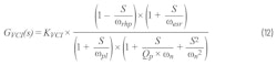
With power components selected, the control-to-output transfer function $G_vc(s)$ for peak current-mode control with internal slope compensation can be modeled. The inner current loop exhibits high bandwidth, permitting the outer voltage loop to be stabilized using a standard Type-II (two-pole, one-zero) compensator.

The power stage transfer function accounts for:

- Low-frequency pole set by the load resistance and output capacitance.
- ESR zero dictated by the output capacitor’s equivalent series resistance ($R_C$).
- RHP zero limiting system bandwidth.
Output capacitance ($C_OUT$) must be properly derated based on the applied negative DC voltage bias. Its value dictates voltage excursions during load steps, while its ESR interacts with the inductor to define dominant power-stage dynamics.
Completing the Converter with a Type-II Voltage-Loop Compensator
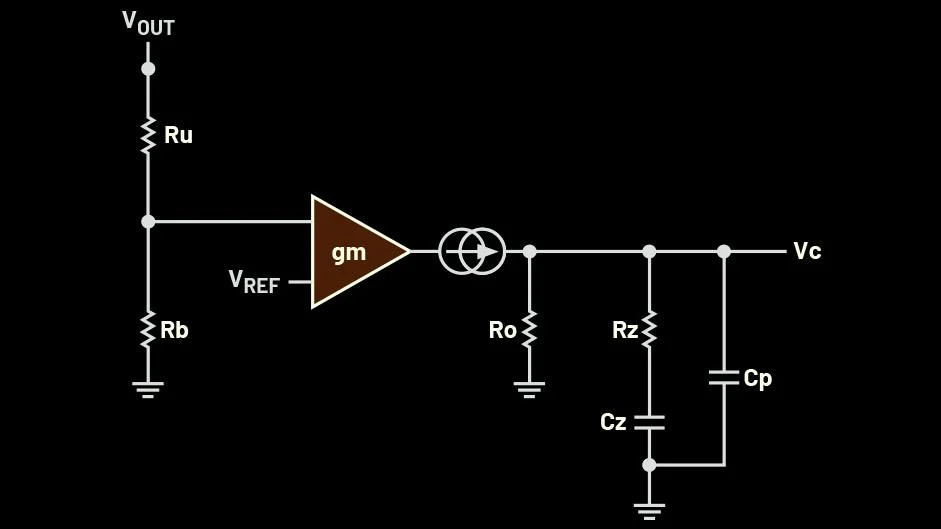
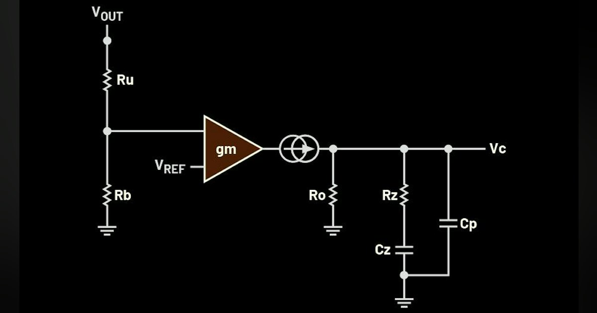
Figure 3 illustrates a classic Type-II voltage-loop compensator configuration utilizing an operational amplifier or error amplifier network. The compensator introduces one zero to boost phase near the crossover frequency and a high-frequency pole to attenuate switching noise.
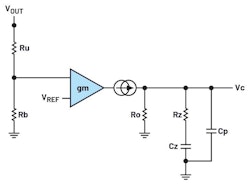
Compensator Design Steps:
- Target Crossover Frequency ($f_c$): Select a crossover frequency well below the RHP zero frequency and roughly 10% to 20% of the switching frequency $f_SW$.
- Calculate Power-Stage Phase Shift: Evaluate the phase angle of the power-stage transfer function at the chosen crossover frequency.
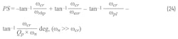
- Determine Phase Boost: For an IBB converter, a healthy phase margin (PM) is targeted above $45^circ$. Selecting a target PM of $60^circ$ defines the required phase boost ($Phi_boost$):
$$Phiboost = PMtarget – 90^circ – textPhase_power_stage(f_c)$$
- Evaluate Design Factor ($k$): Compute the frequency-scaling factor $k$ based on the required phase boost:
$$k = tanleft(fracPhi_boost2 + 45^circright)$$

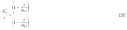
- Locate Compensator Poles and Zeros: Position the compensator zero ($fzc$) and pole ($fpc$) relative to the dominant power-stage pole ($f_p$) and crossover frequency:
$$f_zc = fracfck, quad fpc = k cdot f_c$$

- Calculate Integrator Gain and Component Values: Determine the required feedback resistors, compensation capacitors, and resistors to finalize the Type-II network topology.
Simulation Results and Performance Validation
Simulating the complete inverting buck-boost stage within environments like LTspice confirms theoretical calculations.

- Bode Analysis (Figure 4): Operating at full load with a crossover frequency of approximately $46.27text kHz$, the simulated loop exhibits a Phase Margin (PM) of $59.07^circ$ and a Gain Margin (GM) of $8.90text dB$. While standard design guidelines often target a GM greater than $10text dB$, this slightly lower margin represents an intentional design trade-off prioritizing faster transient response times over strict gain margins.
- Transient Response (Figure 5): Subjecting the converter to a $0.5text A$ to $1.0text A$ load step (with a $0.5text A/mutexts$ slew rate) reveals an output voltage excursion of roughly $2.88%$. This demonstrates tight dynamic regulation and quick recovery times suitable for noise-sensitive instrumentation.
Implications and Engineering Takeaways
Designing a high-performance inverting buck-boost converter for negative-rail generation requires a systematic approach. Inductor selection directly governs the RHP zero location, acting as a natural ceiling for loop bandwidth. Simultaneously, output capacitance selection and ESR management dictate transient voltage excursions and shape power-stage poles.
By systematically deriving small-signal models, accounting for right-half-plane behaviors, and implementing correctly tuned Type-II compensation networks, power electronics engineers can achieve stable, high-bandwidth operation. These verified methodologies ensure that sensitive automotive, industrial, medical, and data center systems receive the clean, reliable negative voltage rails they require.