





Main Facts
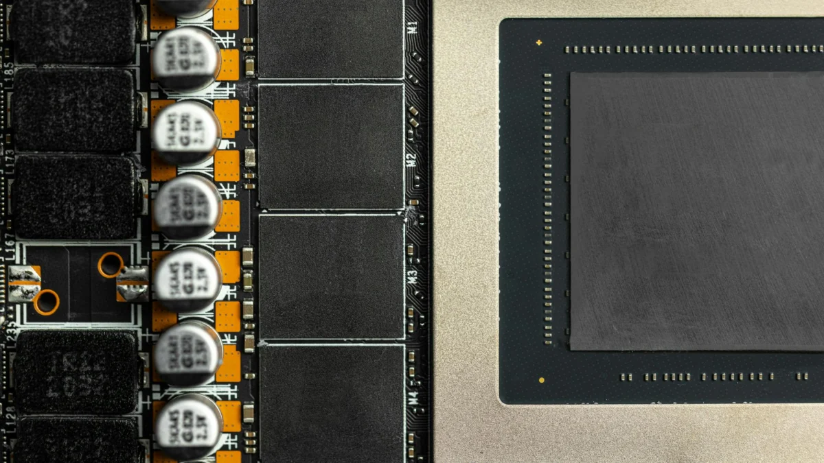
As artificial intelligence models grow exponentially in complexity, the hardware driving them faces a severe physical barrier known as the "power wall." For decades, semiconductor and power engineers have managed processor power from a distance, relying on traditional voltage regulators mounted on motherboards. However, modern GPUs, CPUs, TPUs, and neural processing units (NPUs) now feature thermal design power (TDP) specifications exceeding one kilowatt, with peak power demands reaching multiple kilowatts per chip.
This immense physical separation between legacy motherboard power modules and high-current processors creates critical electrical "friction." The resulting parasitic resistance and inductance cause severe energy loss, extreme heat generation, and voltage droop ($V_drop$) when systems fail to supply current rapidly enough to meet fluctuating workloads.
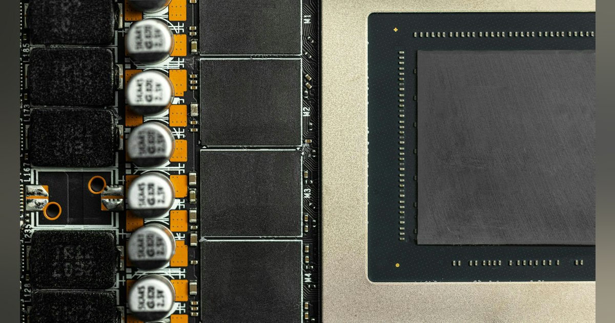
To bypass these systemic limitations, the semiconductor industry is increasingly looking toward Integrated Voltage Regulators (IVRs). By embedding DC-DC converters—including necessary inductors and capacitors—directly inside the AI chip package or onto the silicon die, IVRs place regulation microns away from the processing cores. This proximity dramatically reduces power delivery network (PDN) impedance, enables ultra-high control-loop bandwidths operating at frequencies surpassing 100 MHz, and facilitates granular "micro-island" power management.
According to industry experts like Davood Yazdani, Executive Vice President and Chief Product Officer at Endura Technologies, this paradigm shift requires a fundamental overhaul of traditional chip design, forcing logic and power engineers to collaborate closely via unified co-design platforms.

Chronology
- The Decades of Motherboard-Level Regulation: For generations, compute hardware relied on traditional board-level voltage regulator modules (VRMs) placed inches away from processors. This approach worked well when processor power draws were measured in tens or low hundreds of watts.
- The Rise of the Kilowatt-Class AI Accelerator: As deep learning and large language models (LLMs) scaled, accelerator power demands surged. Modern GPUs broke past the kilowatt threshold, rapidly exposing the severe performance bottlenecks of legacy, board-level power delivery networks.
- The Advent of On-Package and In-Die Integration: Power engineers began experimenting with embedded passives and advanced packaging technologies to move DC-DC conversion closer to the compute engine. This evolution paved the way for commercial IVRs capable of managing high-frequency switching.
- The Modern Co-Design Shift: The industry has moved toward holistic multi-physics design frameworks. Semiconductor firms now utilize standards like Universal Chiplet Interconnect Express (UCIe) and AI-augmented simulation tools to co-design logic and power domains simultaneously from the earliest Register-Transfer Level (RTL) coding phases.
Supporting Data
- Switching Frequencies: Advanced IVR control architectures and power switches operate at switching frequencies exceeding 100 MHz, a massive leap compared to legacy motherboard-level counterparts.
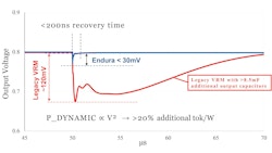
- Transient Response: When subjected to intense workload steps—such as a 1,000-A load step at 75 A/ns—IVRs drastically minimize voltage undershoot and ringing compared to traditional VRMs.
- Thermal and Electrical Constraints: Modern advanced AI accelerators operate at TDP specifications exceeding 1 kW, with peak power demands scaling into multiple kilowatts per individual chip package.
- Granular Efficiency: Instead of utilizing a bulk regulation approach where a single rail feeds hundreds of cores—forcing an over-energized "lowest common denominator" effect—IVRs enable dozens of localized "micro-islands" with dedicated dynamic voltage scaling.
Official Responses
Industry leadership and power management experts have increasingly emphasized that power delivery is no longer a peripheral concern, but a core architectural constraint.
Davood Yazdani, Executive Vice President and Chief Product Officer at Endura Technologies, highlights the necessity of bridging traditional design silos. Yazdani notes that while foundational simulation engines exist, the future of compute relies on closing the gap between power, heat, and logic. "Logic and power can no longer be designed in silos," Yazdani explains, emphasizing that adaptive voltage and frequency scaling (AVFS) relies entirely on the nanosecond execution engine provided by IVRs to capitalize on efficiency opportunities without risking hardware crashes.
Power systems architects across the broader semiconductor ecosystem echo these sentiments, warning that without a transition to high-bandwidth, in-package regulation, future AI performance scaling will be completely capped by fundamental laws of electrical physics.
Implications
1. Reclaiming Dark Silicon and Maximizing AI Efficiency
Traditional power management functions much like a single light switch controlling an entire building, forcing the entire processor die to run at higher voltages to accommodate isolated heavy workloads or localized process variations. IVRs operate more like independent dimmer switches for every room, creating granular "micro-islands."
When paired with adaptive voltage and frequency scaling (AVFS), IVRs react to in-situ critical path monitors in nanoseconds. If an AVFS sensor detects a 10-mV efficiency window, the IVR executes the adjustment instantly. This real-time responsiveness allows chips to reclaim "dark silicon"—areas previously left unpowered or underutilized due to strict thermal and power limits.
2. Physical AI and Next-Generation Robotics
While data centers represent the primary economic driver for IVR deployment, the implications stretch deep into physical AI and autonomous robotics. In robotic systems, power integrity is directly tied to safety and reliability.
When a robot executes high-torque motor movements or processes heavy multi-sensor streams from cameras, radar, and LiDAR, it demands sudden, massive power injections. The ultra-fast transient response and rapid recovery time of an IVR act like a biological reflex, preventing brownouts, erratic movements, or navigation system resets. This ensures that autonomous platforms maintain fluid, reliable movement even under intense computational stress.
3. A Fundamental Restructuring of the Semiconductor Business Model
Perhaps the profoundest implication of the IVR revolution is cultural and structural. Historically, processor architects designed the logic, package engineers mapped out the substrate, and power experts dealt with the motherboard layout independently.
The integration of IVRs shatters these traditional silos. Successful deployment demands a unified co-design model where all three disciplines collaborate from the first line of RTL code. Furthermore, EDA tool vendors are racing to deliver AI-augmented multi-physics platforms capable of automating the optimization of hundreds of independent power domains. Combined with industry-wide adoption of packaging standards like UCIe (Universal Chiplet Interconnect Express), IVRs are fundamentally altering how multi-die chips are architected, packaged, and manufactured for the next generation of computing.