





Main Facts
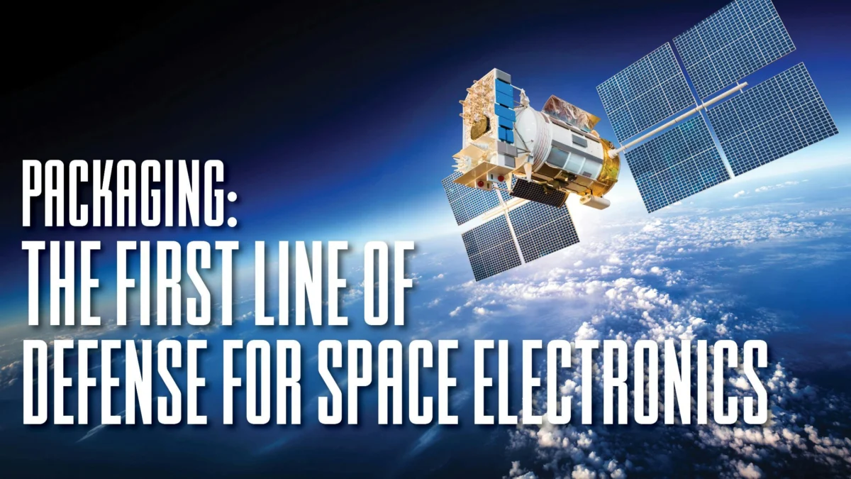
Space is the ultimate stress test for electronics. Beyond the initial violence of a rocket launch—characterized by bone-jarring mechanical vibrations and extreme acoustic resonance—space-bound hardware faces an unrelenting onslaught of cosmic radiation, drastic thermal fluctuations, and the absolute vacuum of the cosmos. For decades, the aerospace industry has focused heavily on the silicon itself, engineering radiation-hardened (rad-hard) microchips capable of withstanding constant bombardment by galactic cosmic rays (GCRs) and unpredictable solar particle events (SPEs).
However, industry consensus has shifted: hardening the semiconductor die at the transistor level is only half the battle.
Today, aerospace engineers recognize that microelectronic packaging—the physical enclosure, interconnects, and thermal management systems that cradle the chip—is equally critical to mission success. Whether a satellite is slated for a brief, multi-year mission in Low Earth Orbit (LEO) or a decades-long deployment in Geostationary Orbit (GEO) or deep space, the integrity of the package dictates the longevity of the entire system.
The modern space economy, defined by the rapid commercialization of "New Space" architectures, mega-constellations, and in-orbit data centers, is driving a revolution in packaging technology. Traditional hermetically sealed ceramic enclosures, while still the gold standard for high-reliability deep-space missions, are being supplemented—and in some cases challenged—by space-qualified plastic packaging designed to dramatically reduce Size, Weight, Power, and Cost (SWaP-C). Simultaneously, breakthroughs in heterogeneous integration, multichip modules (MCMs), and advanced thermal interface materials (TIMs) are solving some of the most persistent engineering challenges in aerospace history, ensuring that tomorrow’s power semiconductors and processing units can survive the harshest environment known to humanity.
Chronology
To understand the current state of space-grade microelectronic packaging, it is necessary to examine how the aerospace industry evolved from customized, artisanal manufacturing to mass-produced commercial constellations.
The Cold War and Early Space Age (1950s–1970s)
During the dawn of the space race, electronics were relatively primitive, and the concept of commercial-off-the-shelf (COTS) components did not exist. Every component destined for a rocket or spacecraft was custom-built, heavily tested, and housed in thick, hermetically sealed metal or ceramic enclosures. Radiation effects such as Total Ionizing Dose (TID) were poorly understood, leading engineers to over-engineer systems with massive safety margins. Packaging during this era was focused almost entirely on mechanical protection and absolute moisture exclusion, as early computers could not tolerate even microscopic levels of corrosion.
The Digital Revolution and Standardization (1980s–2000s)
As integrated circuits advanced, the Department of Defense and major space agencies established rigorous military standards (Mil-Specs) for microelectronics. The QML (Qualified Manufacturers List) system was established to regulate how space chips were designed, tested, and packaged. Hermetic ceramic dual-in-line packages (DIPs) and flatpacks became the undisputed gold standard. During this period, radiation hardening at the semiconductor level (rad-hard by design and rad-hard by process) matured significantly, while packaging largely remained a static, reliable, but heavy and expensive ancillary component.
The "New Space" Paradigm Shift (2010s–Present)
The landscape changed radically with the commercialization of space, spearheaded by private launch providers and satellite internet companies deploying thousands of smallsats into LEO. Traditional hermetic ceramic packaging—often taking months to manufacture and costing thousands of dollars per unit—became a bottleneck. The industry began aggressively adapting consumer-grade plastic packaging for space applications. Concurrently, the demand for higher processing power in orbit forced a move toward dense heterogeneous integration, compelling packaging engineers to reinvent how chips are stacked, connected, and cooled in a zero-gravity, vacuum environment.
Supporting Data
The operational realities of space place extraordinary demands on microelectronic packages. The physical phenomena that packaging must mitigate are quantifiable and severe:
- Radiation Exposure: In LEO, satellites are partially shielded by Earth’s magnetic field, yet they still traverse the South Atlantic Anomaly, a region of intense radiation. In GEO and deep space, devices face uninterrupted solar wind and cosmic rays. TID is measured in kilorads (krad) of silicon; harsh deep-space environments demand components that can withstand upwards of 100 krad to 1 µrad over a 15-year lifespan without suffering catastrophic parametric failure or functional corruption from Single-Event Effects (SEE).
- Thermal Extremes: A satellite in LEO experiences extreme temperature swings every 90 minutes as it moves from direct, unfiltered solar radiation (where exterior temperatures can exceed +120°C) into the shadow of the Earth (where temperatures plummet to -150°C). These rapid thermal cycles induce severe thermomechanical stress at the interface between the silicon die, the substrate, and the package housing, frequently leading to solder fatigue and micro-cracking.
- Mechanical Stress: During launch, multi-stage rockets generate intense acoustic vibrations and high-G acceleration profiles, often exceeding 10Gs to 20Gs of force. Packaging must securely anchor the fragile semiconductor die, preventing internal wire bond shear or substrate delamination under heavy vibration.
- The Thermal Vacuum Paradox: In a terrestrial environment, heat is easily dissipated via conduction and convection through air or fluid cooling systems. In the vacuum of space, convection is nonexistent. All generated heat—particularly from high-power semiconductors used in electric propulsion and power distribution—must be dissipated purely through conduction paths within the package and radiation into deep space via specialized thermal interface materials (TIMs) and radiators.
Official Responses and Industry Insights
Leading aerospace technologists, semiconductor manufacturers, and research institutions have increasingly focused their R&D budgets on advanced packaging innovations.
Dr. Aris Thorne, a senior principal engineer in radiation effects at a major defense contractor, emphasizes that packaging is no longer an afterthought. "Ten years ago, a program manager would spend 95% of their budget on the rad-hard ASIC and assume any standard hermetic box would do the job," Thorne notes. "Today, we realize that a brilliant silicon die can be completely compromised if the package cracks under thermal shock or allows secondary electrons to cascade inward. The package is now an active participant in system survivability."
Meanwhile, commercial entities driving the "New Space" movement are championing plastic encapsulation. Elena Rostova, VP of Materials Engineering for a prominent satellite constellation operator, points to the economic necessity of moving away from traditional methods. "If you are launching a constellation of 4,000 communication satellites, you simply cannot afford the weight, lead times, and financial cost of traditional ceramic hermetic packaging," Rostova explains. "By leveraging advanced plastic-encapsulated microcircuits (PEMs) with specialized underfills and conformal coatings, we have cut our payload packaging costs by over 70% while maintaining acceptable reliability profiles for five-to-seven-year LEO missions."
Thermal management experts also highlight the growing importance of advanced composite materials. According to aerospace packaging consortium whitepapers, the integration of diamond-like carbon (DLC) coatings, advanced copper-molybdenum (CuMo) baseplates, and space-rated phase-change thermal interface materials has unlocked unprecedented power densities for modern in-orbit data centers, enabling kilowatt-class computing architectures that were previously thermally impossible to deploy in space.
Implications
The evolution of space-grade microelectronic packaging carries profound implications for the future of space exploration, global telecommunications, and national security.
Economic Accessibility and the Democratization of Orbit
The transition from artisanal, ceramic-heavy packaging to streamlined, scalable packaging approaches directly lowers the barrier to entry for space exploration. Startups, universities, and emerging spacefaring nations can now deploy sophisticated payloads at a fraction of historical costs. This democratization accelerates scientific research, Earth observation capabilities, and global internet connectivity.
The Rise of In-Orbit Computing
As artificial intelligence, edge computing, and real-time data processing become mandatory for autonomous spacecraft, power semiconductors and high-performance processors must operate reliably in space. Advanced heterogeneous packaging—such as 2.5D and 3D chiplet integration—allows disparate processing, memory, and power management units to be packed into tiny footprints. This yields the high performance required for autonomous collision avoidance, deep-space navigation, and localized data analysis without exceeding strict SWaP-C limits.
Reliability Challenges in Commercial Constellations
However, the pivot toward commercial-grade plastic packaging and accelerated development cycles introduces new risks. Unlike legacy systems designed for 25-year unmaintained missions, many LEO constellations accept a higher failure rate, relying on orbital redundancy. Yet, as space debris becomes an increasingly critical global concern, ensuring that electronic packages do not prematurely fail and create dead, uncontrollable hazards in congested orbits is paramount. Regulatory bodies and international space agencies are beginning to scrutinize whether commercial shortcuts in packaging compromise long-term orbital sustainability.
Conclusion
Ultimately, the future of humanity’s expansion into the cosmos rests not only on the brilliance of silicon engineering but also on the microscopic architecture of the enclosures that protect it. From geostationary sentinels monitoring global weather to deep-space probes hunting for extraterrestrial life, advanced packaging stands as the silent guardian of space-bound electronics, bridging the gap between fragile terrestrial technology and the unforgiving, beautiful void of space.