





By the Editorial Desk
Advanced Manufacturing & Semiconductor Technology Review
Main Facts: The Transition from 2D Inspection to 3D Multi-Modal Characterization
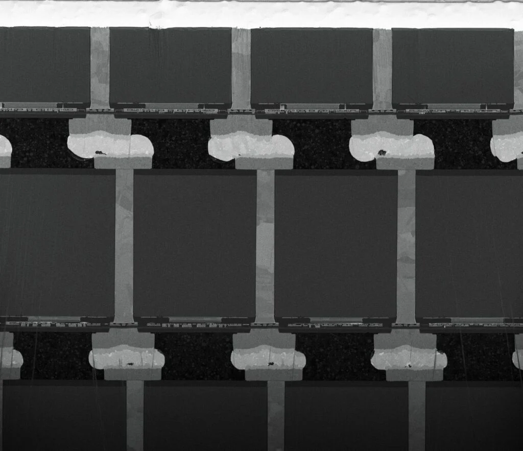
For decades, semiconductor failure analysis operated on a fundamentally two-dimensional plane. Engineers could locate an electrical or physical defect by mapping its X and Y coordinates, slicing open the wafer or die, and identifying the root cause under an electron microscope. However, the relentless pursuit of Moore’s Law—coupled with physical limits on transistor scaling—has driven the industry toward revolutionary design paradigms. Today, advanced logic, dense memory architectures, and massive artificial intelligence (AI) hardware rely heavily on 3D stacking, heterogeneous integration, chiplet configurations, and sophisticated through-silicon via (TSV) networks.
According to industry experts, this architectural evolution has transformed failure analysis from a localized 2D task into a complex 3D challenge. As Dr. Mohan Iyer, Vice President and General Manager of Semiconductors at Thermo Fisher Scientific, points out, understanding depth (the Z-axis) is now just as critical as determining surface coordinates. Modern semiconductor packages combine multiple active dies, hybrid bonds, redistribution layers (RDLs), and intricate power delivery networks into single, highly integrated units.
When an electrical failure occurs in these multi-die environments, the root cause may originate in one active layer yet manifest entirely elsewhere in the package. This high degree of integration makes traditional monolithic failure analysis methods obsolete. Consequently, fabrication facilities (fabs) and outsourced semiconductor assembly and test (OSAT) providers are overhauling their diagnostic workflows, integrating plasma focused ion beam (PFIB) milling, multi-modal imaging, artificial intelligence, and fab-proximate metrology to maintain high manufacturing yields and profitability.
Chronology: The Evolution of Semiconductor Diagnostics
To understand the urgency driving the adoption of 3D failure analysis, it is necessary to examine how semiconductor design and diagnostic methodologies have evolved over time:
- The 2D Era (1980s–2010s): Semiconductor manufacturing focused primarily on planar CMOS scaling. Devices were built on single monolithic dies. Failure analysis was largely straightforward, relying on optical inspection, basic mechanical cross-sectioning, and 2D scanning electron microscopy (SEM) to find localized short circuits or open circuits on the surface or in shallow subsurface layers.
- The Advent of 3D Stacking and TSVs (2010s–Early 2020s): As horizontal scaling slowed, the industry moved upward. Through-silicon vias (TSVs) and early 3D-IC packaging were introduced to connect stacked memory and logic chips. Failure analysis began facing visibility challenges, requiring specialized focused ion beam (FIB) techniques and X-ray imaging to peer beneath upper layers.
- The Heterogeneous Chiplet and AI Era (Present Day): Modern high-performance computing (HPC) and generative AI accelerators demand massive compute power, leading to heterogeneous chiplet architectures. Devices integrate logic, high-bandwidth memory (HBM), and power management integrated circuits (PMICs) onto advanced interposers or through hybrid bonding. Failure analysis has fully transitioned into a multi-modal, 3D discipline where buried structures, interface delamination, and sub-surface TSV misalignments require advanced automated workflows and plasma-based milling tools.
Supporting Data and Technical Complexities
The shift toward 3D architectures introduces profound technical hurdles that directly impact manufacturing yields, time-to-market, and overall production costs.
The Multi-Material and Interface Challenge
Modern advanced packages are not merely dense; they are chemically and structurally diverse. They combine silicon, copper interconnects, organic substrates, wide bandgap semiconductors (such as Gallium Nitride, or GaN, used in power electronics), and various encapsulation polymers. Each material responds differently to thermal, mechanical, and electrical stresses.
Failure analysis engineers must now navigate complex interactions across multiple interfaces that were previously evaluated in isolation. Subtle variations at a single buried interface—such as micro-voids, copper pump-out, or thermal coefficient of expansion (TCE) mismatches—can compromise the long-term reliability of the entire device.
The Multi-Modal Data Dilemma
Because no single analytical technique can reveal the full picture of a buried defect, engineers must rely on a battery of complementary methods:
- X-ray Microscopy (XRM) and Acoustic Imaging: Used for non-destructive bulk inspection to locate anomalies, voids, or delamination within encapsulated packages.
- Plasma Focused Ion Beam (PFIB) Milling: Essential for rapidly removing large volumes of material to expose deep sub-surface structures like TSVs with minimal curtaining artifacts.
- Electron Microscopy and Chemical Analysis: Provides high-resolution structural and compositional data of defect sites.
- Infrared (IR) and Electrical Characterization: Pinpoints thermal anomalies and functional electrical failures before destructive physical analysis begins.
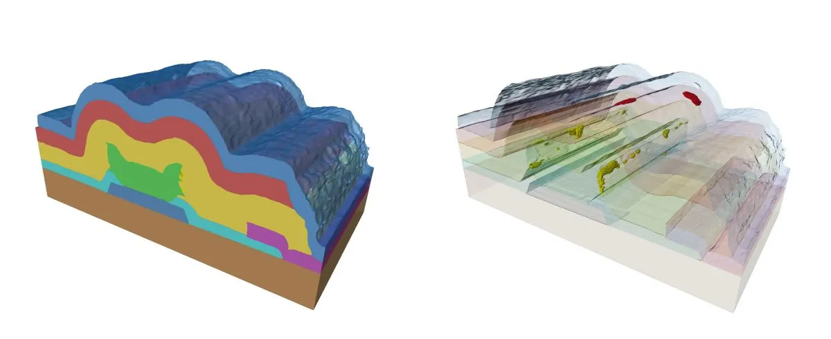
However, each of these techniques generates massive amounts of data with disparate resolutions, coordinate systems, and contrast mechanisms. Correlating these multimodal datasets into a unified, three-dimensional representation requires sophisticated software workflows that preserve spatial accuracy across techniques.
Official Perspectives and Expert Insights
Industry leaders emphasize that the economic pressures surrounding advanced nodes—particularly for AI hardware—leave little room for prolonged diagnostic cycles. AI chips are physically larger, vastly more expensive to manufacture, and subject to intense thermal and electrical loads.
"Failure analysis is therefore becoming more than simply a laboratory function," explains Dr. Mohan Iyer. "This is especially true for AI chips because of their larger size and high manufacturing costs. Identifying failures early in the process is imperative to maximising yield and profitability."
When yield excursions occur, delays in identifying root-cause mechanisms slow down process optimization and corrective actions. In an industry where multi-million-dollar production lines run around the clock, extended learning cycles can cost companies millions of dollars in scrapped wafers and missed market windows.
To mitigate these risks, the semiconductor ecosystem is decentralizing failure analysis. Traditionally conducted in isolated, centralized analytical laboratories far removed from the production line, advanced metrology and sub-surface defect analysis are now moving closer to the cleanroom floor. By bringing analytical capabilities nearer to the fab, process engineers receive faster feedback, enabling rapid corrections that prevent systemic yield loss.
Implications: The Future of Yield Optimization and AI Integration
The transition to full 3D failure analysis carries profound implications for the future of semiconductor manufacturing, software development, and workforce dynamics.
The Role of Artificial Intelligence and Workflow Automation
As the volume and complexity of analytical data skyrocket, human expertise alone is no longer sufficient to process information in real time. Artificial intelligence and machine learning are stepping in not to replace expert analysts, but to augment their capabilities.
Machine learning algorithms are increasingly deployed to:
- Identify subtle, recurring defect signatures hidden deep within multi-terabyte datasets.
- Automate image segmentation for complex structures, such as Gallium Nitride High-Electron-Mobility Transistors (GaN HEMTs) requiring intricate 3D reconstruction.
- Simplify cross-modal registration, allowing engineers to seamlessly overlay X-ray, acoustic, and electron microscopy data.
By automating repetitive data-preparation tasks, AI lowers the barrier to entry for advanced characterization tools. Process and yield engineers can access sophisticated diagnostic insights without requiring decades of specialized sample-preparation experience. Senior experts are thereby freed from manual data manipulation, allowing them to focus entirely on high-level interpretation and root-cause resolution.
Beyond Transistor Scaling
Ultimately, the primary bottleneck in semiconductor innovation is no longer just the ability to shrink transistor gates; it is the ability to effectively utilize diverse analytical information to ensure package reliability. As the industry relies increasingly on advanced packaging innovations to drive performance gains, failure analysis will serve as the foundational enabler of yield improvement.
The evolution from 2D surface inspection to multi-modal 3D analysis—underpinned by plasma focused ion beam milling, AI-assisted workflows, and fab-proximate data delivery—will dictate which semiconductor manufacturers successfully scale the next generation of high-performance computing and artificial intelligence infrastructure.